Silica Management Solutions for Semiconductor Companies

The semiconductor industry’s pursuit of smaller, faster, and more powerful chips demands ultrapure water. Achieving this level of water purity presents water management challenges, making silica management solutions for semiconductor companies crucial. From high water usage to stringent regulations, semiconductor companies face several water treatment process complexities.
How can semiconductor manufacturers achieve the necessary water purity for chip production? How can they manage the resulting wastewater?
This article explores effective silica water treatment management solutions for semiconductor companies. It also highlights how these solutions promote responsible water systems and environmental sustainability.
Table of Contents:
- The Water Challenge in Semiconductor Manufacturing
- Silica: A Tiny Troublemaker
- GCAT: A Game-Changer in Pretreatment
- Reverse Osmosis: Polishing the Water
- Wastewater Management: Closing the Loop
- Silica Management Solutions for Semiconductor Comp: A Holistic Approach
- FAQs about silica management solutions for semiconductor comp
- Conclusion
The Water Challenge in Semiconductor Manufacturing
Computer chip manufacturing is water-intensive. A large semiconductor fabrication facility (fab) can use millions of gallons of water daily. For example, a fab processing 40,000 wafers monthly might use up to 4.8 million gallons per day.
This is comparable to the annual water usage of a city with 60,000 people. About 75% of this water directly supports manufacturing processes. Even tiny impurities can damage chips, so creating ultrapure water requires advanced water treatment technologies.
Silica: A Tiny Troublemaker
Silica, a common water contaminant, poses a significant challenge. Even small silica particles can disrupt chip manufacturing, sticking to components and causing defects. Silica also forms scale in pipes and equipment, reducing efficiency and lifespan.
Removing silica from raw water is a complex process. It requires industrial water treatment solutions that use multiple methods.
GCAT: A Catalytic Innovation in Pretreatment
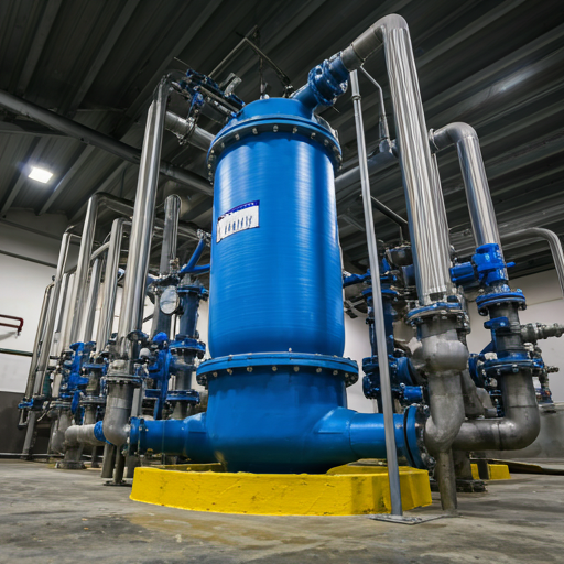
Genesis Catalytic Activation Technology (GCAT) is a leading pretreatment technology for silica reduction. The catalytic treatment media enhances silica precipitation.
This simplifies silica remediation before it reaches reverse osmosis (RO) membranes, reducing silica loading on downstream equipment. GCAT offers several advantages.
It functions effectively even at low total dissolved solids (TDS) levels and minimizes chemical use, increasing permeate recovery rates while making it more environmentally friendly than other pretreatment options.
The G-CAT system effectively neutralizes and alters the molecular structure of dissolved silica through its catalytic treatment media, proving particularly useful for industrial feedwater sources with varying TDS concentrations.
Reverse Osmosis: Polishing the Water
After GCAT pretreatment, reverse osmosis (RO) polishes the water for ultrapure water production. Reverse osmosis removes over 95% of dissolved silica, making it essential for wafer rinsing and cleaning.
Combining GCAT and high-efficiency reverse osmosis with antiscalants benefits semiconductor fabs. Producing 1,000 gallons of ultrapure water requires 1,400 to 1,600 gallons of municipal water.
GCAT combined with small doses of specific antiscalants prevent silica from fouling RO membranes. This extends membrane life, prevents scaling, and reduces the need for harsh cleaning chemicals. Improved permeate flow rates also lower operational expenses and wastewater generation.
Wastewater Management: Closing the Loop
Silica water treatment and management extends beyond clean water production to wastewater treatment. Semiconductor manufacturing generates substantial wastewater.
This water requires careful treatment before discharge or reuse. With tightening regulations, the semiconductor industry is increasing adopting innovative and sustainable solutions.
Zero or minimal liquid discharge solutions optimizes water recovery and minimizes wastewater discharge.
Silica Management Solutions for Semiconductor Companies: A Holistic Approach
Semiconductor companies are adopting a holistic approach to silica water treatment management. Effective solutions begin with preventative strategies, such as process optimization and pretreatment with systems like GCAT.
High-efficiency RO systems improve efficiency and reduce environmental impact. Responsible and sustainable wastewater treatment is crucial.
Water scarcity is a growing concern. Investing in robust management solutions addresses cost pressures from stricter discharge regulations and limited water supplies.
Regulations are tightening with greater emphasis on responsible environmental stewardship, especially for the semiconductor industry’s liquid discharge and water recovery needs.
Effective semiconductor water treatment impacts every step of the process. Companies look for high water recovery and increased recovery rates to offset operational expenses, making Electro-deionization systems a common industrial post polishing water treatment system, a crucial aspect of this equation.
Using effective, sustainable industrial water treatment methods can provide a simple process that leads to innovative solutions.
Implementing advanced water treatment processes requires planning and foresight, however the impact semiconductor manufacturers have by utilizing such processes can minimize environmental impact as well as mitigate issues such as scaling and mineral buildup, which can damage equipment.
Therefore, improving water processes and minimizing these potential hazards is imperative to high quality outputs. While optimizing water usage and investing in innovative solutions such as membrane bio-reactor (MBR) technology and high efficiency RO with high recovery can reduce capital costs over time, semiconductor water treatment is a key aspect that must be considered, designed, and executed for water purification purposes.
Conclusion
As semiconductor companies strive for technological breakthroughs, addressing their unique water management challenges is more crucial than ever. Advanced silica water treatment management solutions for semiconductor companies empower manufacturers to achieve the ultrapure water essential for chip production while efficiently managing wastewater.
By leveraging innovative systems like GCAT and high-efficiency reverse osmosis, these solutions not only ensure compliance with stringent regulations but also promote sustainable practices that conserve water resources.
Investing in such technologies minimizes environmental impact and operational costs while safeguarding the quality and longevity of manufacturing equipment.
To explore how your semiconductor operations can benefit from cutting-edge pure water and wastewater treatment solutions,
Contact the water specialists at Genesis Water Technologies today at +1 321 280 2742 or via email at customersupport@genesiswatertech.com to take the first step towards smarter water management tailored to your needs.
FAQs about silica management solutions for semiconductor companies
How to reduce silica in water treatment?
Several methods can reduce silica in water treatment, including lime softening, catalytic activation treatment (like GCAT), reverse osmosis, and electrocoagulation.
Effective silica removal depends on factors such as source water quality, target silica levels, and application.
Combining different technologies may provide more thorough silica removal, allowing treatment process customization.
How is water used for in the semiconductor industry?
Water in the semiconductor industry serves several crucial functions. It cleans and rinses wafers, cools equipment, and plays a role in power generation.
Ultrapure water is essential for wafer fabrication. Reclaimed water can be used for other process applications. Water reuse programs reduce water footprint and lessen the burden on water resources.
What is silica in water treatment?
Silica in water treatment refers to forms of silicon dioxide (SiO2), a natural compound found in many water sources. Silica forms scale on surfaces, impacting industrial water treatment systems.
Remediation of silica from water systems protects equipment and ensures smooth operation, improving treatment systems for removing silica and leading to greater longevity of pipes and machinery.
How much water does a semiconductor plant consume?
While water use per chip is minimal, a chip manufacturing facility’s total water consumption can be substantial. A fab processing 40,000 wafers per month could use around 4.8 million gallons of water daily.
This is roughly equivalent to the annual water usage of a 60,000-person community, showcasing the high water demands of the industry.

